
Flexible and stretchable devices are a fast-growing class of technology that has the potential to revolutionise life by pioneering;
- Healthcare applications
- The interaction between humans and machines
- Internet of Things
- Other applications.[1]
In most cases, flexible printed circuit (FPC) issues arise because the designers are more accustomed to designing rigid circuit boards, so they design flex circuit boards according to the same principles. Of course, flex circuit boards are not rigid circuit boards, and they require their own flex-friendly design.
Flexible Material Selection
Flexible Materials can be divided according to the different functions of materials in flexible electronic devices, they can be divided into basic substrate materials, conductive materials, semiconductor materials, dielectric materials, etc. Flexible material in addition to considering the optimization of device performance, the selection of materials must also fully consider the requirements of the assembly process on material performance to achieve low manufacturing costs.
Base Materials
To meet the requirement of flexible electronic devices, the base material must have a number of attributes. It must be bendable but not fragile, impact resistant, high insulation and cost effective.
Roll-to-roll printing technology (R2R) is a fabrication method used in manufacturing that embeds, coats, prints or laminates varying applications onto a flexible rolled substrate material as that material is fed continuously from one roller on to another. In addition, you can also use R2R to greatly increase productivity and reduce production costs. Accounting for the above considerations, high molecular polymers are most used for flexible substrates. The common flexible substrate materials include polyimide, polyethylene naphthalate (PEN), polymer organic polymers such as polyester (PET) [2], these organic materials can meet the requirements of insulation, flexibility, and strength well.
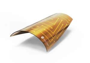
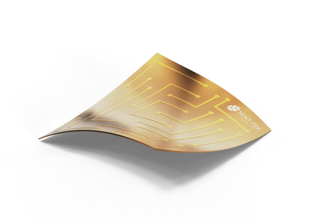
Fig. 1 artistic impression of a flexible electronic device prepared on a polyimide plastic substrate.
In this article, we will be looking into the following aspects of the FPC design:
- Flexibility and number of layers of FPC
- Flexible PCB traces
Flexibility and number of layers of FPC
Keeping the following in mind are very helpful during the design phase;
–Knowing the number of times your FPC will bend is crucial to your design. If a PCB is bent more times than the design allows for, the copper will begin to stretch and crack. Bend radius is the minimum amount the flex area can bend.
-Keep the number of layers as low as possible
-The standard stiffener thickness varies from 0.002′′ to 0.059′′. The FR-4 stiffeners can be 0.008″ to 0.059″ thick while the Kapton stiffener thickness ranges from 0.002″ to 0.010″. The more support the PCB stiffener provides, the thicker it is. Each design requires a distinct thickness.
-Avoid to solder joints not too close to bend point
-Add flexibility to bend the radius of the circuit at the intersection of rigid and flex parts. This will avoid the stress on the flex part during multiple bending operations.
Flexible PCB traces
The following points are also important;
-The performance and longevity of a FPC can be directly attributed to the layout of the circuitry. Signals should never be routed at sharp angles. Mint-Tek recommends the largest radius possible for your design when designing multi-layer FPC, stagger traces on the front and back.
-Avoid sharp corner traces, curved traces are more efficient.
-In a FPC, a trace entering a pad forms a weak spot in which the copper might get fatigued over a point of time. It is always recommended to taper down the pads towards (as shown below) the end in which they are connected to the traces.
-Support for pads on FPC. Copper is prone to be detached from the substrate due to the bending of the flex circuit. It is vital to provide mechanical support for the exposed copper. The through-hole plating in the vias inherently provides mechanical support to the vias in the flex region. Additional through-hole plating of up to 1.5mils is recommended for rigid-flex and FPC.
-Keep certain areas of flexible circuits flat and stable.
-Ensure compliance with ZIF connector specifications.
| layer count: | 1-6 | |
|---|---|---|
| PI core thickness: | 12.5um ,25um , 50um | |
| Board thickness tolerance : | flex :±0.03mm, PI stiffener area :±0.05mm , FR4 stiffener area :±0.1mm | |
| Stiffener: | Yes (PI stiffener , FR4 stiffener ) | |
| stiffener position tolerance : | ±0.2mm | |
| Board size: | min 15*20mm, max 250*800mm | |
| finished copper thickness : | outer :0.5oz-1.5oz , inner :0.5-1oz | |
| min drill bit : | 0.15mm (normal :0.2mm min) | |
| hole size tolerance : | ±0.05mm | |
| cover lay : | yellow ,black ,white (can print solder mask ink) | |
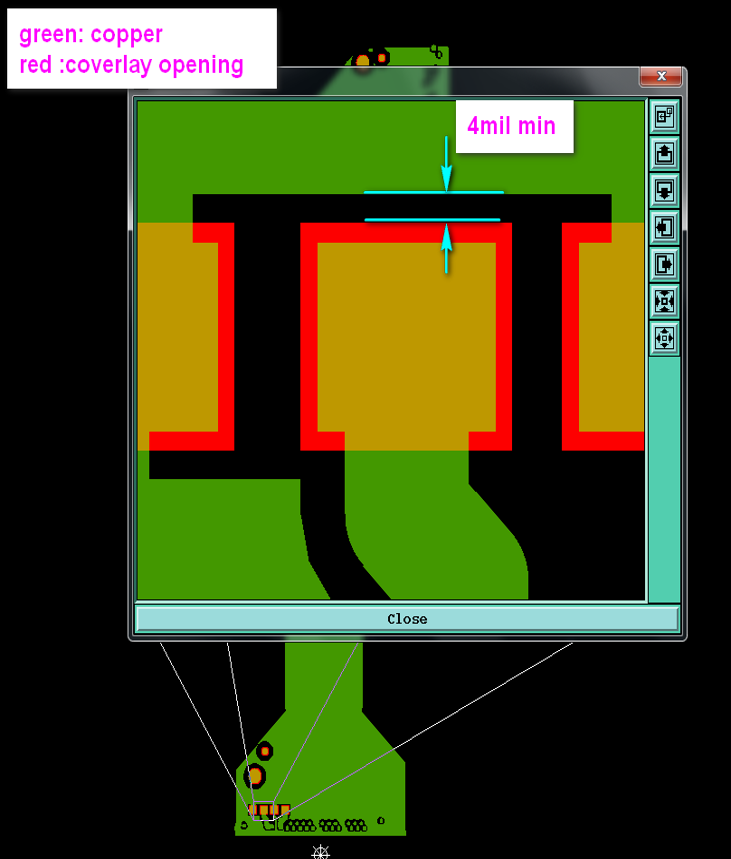
| cover lay opening bigger than pad : | 4mil min for all directions | Pic. 1 |
| cover lay opening to trace or copper: | 4mil min | Pic. 2 |
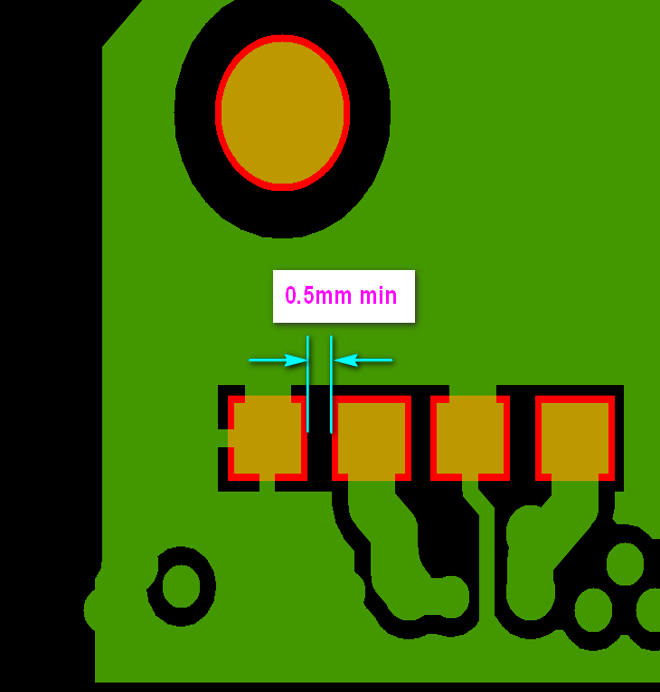
| space between cover lay opening(mould cut ) : | 0.5mm min | Pic. 3 |
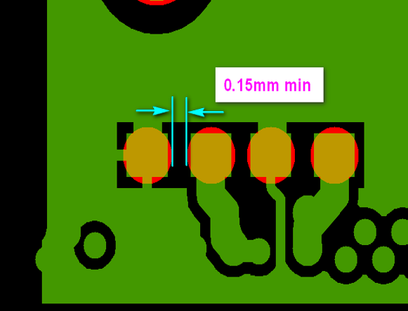
| space between cover lay opening(drill out, shape is round ) : | 0.15mm min | Pic. 4 |
| cover lay opening size (mould cut): | square: 0.8*0.8mm min, oval : width 0.8mm min, round :0.8mm min | |
| min annular ring : | 4mil | |
| min trace width/spacing : | 2.5/2.5mil min (copper 0.5oz) , 3.5/3.5 mil min (copper 1oz), 5/5.5mil min (copper 1.5oz) | |
| via pad to trace : | 4mil min | |
| trace width tolerance : | ±20um (width less than 0.1mm) , (more than 0.1mm , tolerance ±20%) | |
| copper to board edge: | 10mil min | |
| no plated holes to copper or trace : | 10mil min | |
| board dimension tolerance : | normal ±0.13mm , ±0.1mm (length less than 50mm) , | |
| min routing width : | 0.8mm | |
| surface finish : | ENIG (AU:1u''min, 2u''min , Ni:80-200u'') plating hard gold( AU:3-5u'' ,Ni:80-320U'') OSP | |
| impedance control: | yes,(50-100 ohm, tolerance ±10% ) | |
| 3M tape : | yes | |
| .............................. | .............................. | .............................. |
 |  |  |  |
|---|
Replacing Components
Replacing components on a flex only circuit can result in lifted and or torn SMT and PTH pads. Depending upon the flex core type used the copper is either adhered to the Polyimide core with a layer of adhesive or the Polyimide is cast on to the copper. With either configuration, an excessive or repeated application of soldering level temperatures may cause the copper pad to detach from the underlying adhesive or polyimide. Care must be taken not to overheat the solder joint(s) and not to repeatedly rework the same circuit.
Conclusion
The global flexible electronics and organic electronics industry are estimated to increase upwards by $75 billion by 2027, according to the world market research report. Flexible electronics continue to evolve every day, so the future of flexible electronics includes its adoption into an abundance of new applications. New research is driven by functional materials with incredible new methodologies of fabricating devices that are rugged, lightweight, low-cost to produce, with specific electronic and mechanical properties.
Flexible PCB design errors can be avoided by ensuring the manufacturability of your idea at the prototype stage. Talk to your manufacturer and ask their advice.
Spending that extra bit of time on the early stages of design could help mitigate issues and reduce costs in the long run. Paying close attention to the complexity of the FPC application as well as the capabilities and recommendations of your supplier.
GET IN TOUCH
To learn more about how Mint-Tek can meet all your FPC needs for your applications, please make an enquiry with us.
References
- Luan H, Zhang Y (2021) Programmable stimulation and actuation in flexible and stretchable electronics. Adv Intell Syst. https://doi.org/10.1002/aisy.202000228
- MacDonald WA, Looney MK, MacKerron D et al (2007) Latest advances in substrates for flexible electronics. J Soc Inf Disp 15:1075. https://doi.org/10.1889/1.2825093